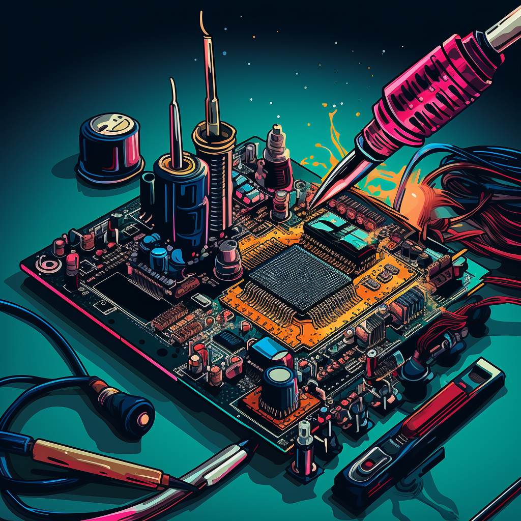
Printed Circuit Board Soldering (PCBs Part 2)

The first major step of PCB assembly is the application of the solder paste. Solder paste is a mixture of ultrafine powdered solder mixed with liquid flux. Solder is used to establish an electrical bond between components. Flux, when heated, burns away corrosion and contamination while also promoting the improved flow of the solder during heating.
Solder paste is applied by placing a stencil mask on the PCB and then wiping paste across the mask such that it is applied only in the desired areas of the PCB. Normally wiping is accomplished using an automated squeegee system. Correct solder volume is critical to ensuring an adequate electrical bond. Design engineers must ensure that stencils have proper depth and spacing to promote sufficient solder paste adhesion to the board.
Once solder paste has been applied to the board, the pick-and-place machine uses a vacuum cup to move components from specially mounted tape reels onto the board. Component tubes or trays may also be used; however, this method of component storage should be avoided whenever possible due to the increased chance of component nesting or tangling before being captured by the pick-and-place.
If proper solder paste application has been accomplished, components should immediately adhere to the paste when placed there by the pick-and-place machine. If component adhesion is insufficient, modifications to the build sequence should include a stage in the pick-and-place cycle where the adhesive is applied to the component.
Engineers also must work to ensure that designs maximize the capabilities of the pick-and-place machine by avoiding through-hole components in favor of surface mount devices whenever possible. Pick-and-place machines generally only work with SMD components due to the wide variability of sizes and shapes in through-hole components. As the pick-and-place machine will take the same time to set up for a handful of PCB board runs as it would for thousands, consideration should be made for grouping production runs together to minimize retooling times.
Pick-and-place machines are also limited by the number of component reels they support. Typical machines may hold between 20 to 100 reels, depending on the tooling style. If a PCB is designed with more unique component models than the pick-and-place machine supports, either additional tooling will be required, or the pick-and-place machine must be reset to do additional component runs.
The number of unique components in use for a given PCB can be minimized through design decisions. Resistor types may be reduced by placing existing resistors in series or parallel to eliminate an infrequently used resistor type. Surface mount fuses may be standardized across the board to reduce the number of fuse sizes in use. Fuses should never be resized in a manner that will prevent proper protective action from occurring, however.
Similar to resistors, capacitors and inductors may also be added in series and in parallel to create the desired capacitance or inductance to reduce the number of unique component types in use; however, some consideration should be given to cost as these components are more expensive than resistors.
As an additional consideration related to reel cost, particular concern should be paid during low-volume production runs for especially expensive components such as GPS modules or accelerometers. These component reels may run many thousands of dollars for reels composed of a thousand components. If the production run only uses a fraction of the reel, the component should instead be assembled by hand using components from a cut tape rather than by a pick-and-place using a full-sized reel.
Once all of the components are on the board, solder reflow may begin. This is the process by which solder paste is melted in an oven to form electrical bonds in all applicable areas. Engineers must design the reflow cycle such that thermal transients are minimized while still providing sufficient heat to activate and subsequently vaporize the heat flux.
The reflow cycle must also adequately transition the solder to a liquid state and then solidify it in a single structure to bind the component to its associated location permanently. Thermal shock must be avoided as that will lead to premature failure. The flux must have sufficient time to evaporate, or excessive aqueous washing may be necessary to clean the board. Sufficient soak time must be provided for proper heat propagation throughout the board to ensure an adequate solder bond.
PCB Manufacturing Series:
Part 1: General Design
Part 2: Soldering and Placement
Part 3:Finishing Processes
Part 4: Testing
References:
Cohen, A., 2015, Prototype to Product: A Practical Guide for Getting to Market, O'Reilly, Boston, USA.
Shina, S., 2008, Green Electronics Design and Manufacturing: Implementing Lead-Free and RoHS-Compliant Global Products, McGraw-Hill, New York, USA.
Hubing, T., Hubing, N., 2016, Not-So-Good EMC Design Guidelines,†from http://learnemc.com/not-so-good-emc-design-guidelines
Yates, R., 2014, Probability and Stochastic Processes, Wiley, Danvers, WA, USA.


Member discussion